
PCBA Capabilities
Shenzhen Tengmei Technology Co., Ltd. is a Shenzhen-based PCBA contract manufacturer. The tables below document the assembly window our factory holds today — surface-mount, through-hole, inspection and test, component sourcing, and the bare boards we supply into that process — so your engineering team can check a design against real limits before requesting a quote.
Standard and advanced assembly windows
Two tiers are quoted separately because they run on different process controls. Standard covers the overwhelming majority of production orders and is priced from the automated line. Advanced covers finer pitch, tighter placement accuracy and specialised materials, which are routed through engineering review and may extend lead time.
Kitted and programmed within a day when files and stock parts arrive before 14:00 CST. Ideal for design iterations, pilot builds and repeat orders on an unchanged revision.
Reviewed by a process engineer before quotation. Used for 01005 parts, 0.35 mm pitch, cavity-up PoP, press-fit connectors and Class 3 inspection regimes.
SMT assembly — standard vs advanced
| Item | Standard capability | Advanced capability | Remarks |
|---|---|---|---|
| Minimum component size | 0201 (0.6 × 0.3 mm) | 01005 (0.4 × 0.2 mm) | Passive placement verified by 3D AOI |
| BGA ball pitch | 0.50 mm | 0.40 mm (0.35 mm on request) | Every BGA lot radiographed |
| CSP / PoP pitch | 0.50 mm | 0.40 mm, package-on-package | Stacked die assembly with spacer check |
| QFN / DFN lead pitch | 0.50 mm | 0.35 mm | Thermal pad aperture tuned per paste volume |
| Fine-pitch leadframe (SOP/TSOP) | 0.4 mm | 0.3 mm | Lead coplanarity checked off-line |
| Placement verification | 01005 passives | 0.3 mm minimum IC pitch | Verified on every first article by 3D AOI |
| Placement throughput | 2,000,000 points per day | across all eight lines | Stated per day, because that is how jobs are scheduled |
| Maximum board size | 800 × 480 mm | Larger panels quoted on request | Panelisation agreed at DFM stage |
| Minimum board size | 50 × 50 mm with breakaway | 10 × 10 mm single board | Carrier fixture for boards below 50 mm |
| Board thickness range | 0.8 – 3.2 mm standard | Thinner stock run on a carrier | Confirmed against the stackup at DFM |
| Board layer count | Set by the board fab | 1 – 32 layers typical | Layer count is a fab decision, not an assembly limit |
| Component height | up to 25 mm | up to 30 mm | Tall parts placed last to avoid nozzle clash |
| Feeder positions | 120 per line | 240 across dual-lane setup | Reel barcode bound to machine program |
| Solder paste | SAC305 lead-free, Type 4 | Type 3 / Type 5 for fine aperture | Lead-containing process available on request |
| Stencil | Laser-cut stainless, 0.10 – 0.15 mm | Electropolished, nano-coated, step stencil | Aperture area ratio reviewed above 0.66 |
| Reflow | Lead-free, SAC305 | Profile run on a coupon each shift | Thermal profile archived per product |
| Changeover | Quoted per build | Feeder carts pre-kitted between jobs | High-mix scheduling is the default, not the exception |
| Production lines | 8 lines | Yamaha YSM20 / YSM10 | Eight lines in parallel, not one line with extra heads |
| Minimum order quantity | 50 pieces | Smaller runs reviewed case by case | No tooling charge on an unchanged revision |
| Standard lead time | 3 working days | Standard build, parts in stock | Component lead time excluded and flagged at quote |
Values are production limits, not marketing targets. Anything outside the advanced column is quoted individually after engineering review.
THT, mixed technology & box build
| Item | Standard capability | Advanced capability | Remarks |
|---|---|---|---|
| Through-hole insertion | Manual, guided by optical template | Automated radial / axial sequencing | Mixed-technology boards run in one flow |
| Wave soldering | Dual-wave, lead-free | Nitrogen-shielded dual-wave | Pallet design included in NRE |
| Selective soldering | Programmable single nozzle | Multi-nozzle with nitrogen | Preferred for connectors near SMT parts |
| Press-fit connectors | Pneumatic press, load monitored | Servo press with force-distance curve | Curve stored per connector type |
| Hand soldering | Workmanship to IPC-A-610 | Class 3 build on request | Iron tips temperature-checked daily |
| Wire & harness assembly | Cut, strip, crimp, tin | Custom overmoulding and harness test | Pull-force sampled per lot |
| Conformal coating | Manual spray or dip | Robotic selective coating | IPC-CC-830 acrylic, silicone, urethane |
| Potting & encapsulation | Two-part epoxy or polyurethane | Vacuum degassing before cure | Bubble inspection after cure |
| Underfill / edge bond | Manual dispense | Jet dispense with X-ray verification | Used on drop-sensitive BGA |
| Enclosure integration | Board into customer-supplied housing | Full box build with incoming enclosure inspection | Torque and screw records retained |
| Labels & serialisation | Printed label, manual application | Automated print-and-apply with serial binding | Serial linked to test log |
| Retail packaging | Bulk ESD bag and carton | Custom insert, accessory kit, retail-ready pack | Drop test on request |
| Sub-assembly test | Continuity check | Full functional test after box build | Firmware version recorded per unit |
| Standard lead time | 5 – 8 working days | 8 – 15 working days for box build | Depends on enclosure supply |
Inspection & test
| Item | Standard capability | Advanced capability | Remarks |
|---|---|---|---|
| Solder paste inspection | Inline 2D SPI | Inline 3D SPI (height / area / volume) | Out-of-limit prints washed and reprinted |
| Pre-reflow AOI | Sampled | 100% on fine-pitch and BGA products | Catches placement offset before scrap |
| Post-reflow AOI | 100% 3D AOI | Dual-camera 3D, 30 mm component height | First and last article images retained |
| X-ray inspection | 2D, sampled by lot | 3D CT, 100% on BGA and QFN | Void percentage reported against IPC-7095 |
| BGA void acceptance | Reported against IPC-7095 | Per ball, not averaged across the package | Out-of-spec lots are reworked or scrapped, not shipped |
| In-circuit test | Not in-house | Fixture and program built with a qualified partner | Quoted as a separate line item when ICT is required |
| Functional test | Custom jig with manual sequence | Automated sequence with data logging | Test coverage signed off before production |
| Firmware programming | Manual or single-gang programmer | Gang programming with checksum verification | Version bound to serial number |
| Boundary scan / JTAG | On request | Automated chain test | Requires customer BSDL files |
| Burn-in / thermal cycling | Ambient soak | −40 °C to +85 °C chamber, logged | Duration defined per product |
| Optical microscopy | Sampled visual inspection | Stereo microscope on every first article | Images attached to FAI report |
| Quality documentation | CoC + FAI report | Per-lot device history record | Retention period agreed per customer |
Component sourcing & compliance
| Item | Standard capability | Advanced capability | Remarks |
|---|---|---|---|
| Authorised channels | Franchised distributors and factory allocation | Second-source proposal in writing | No open-market brokers used |
| Certificate of conformance | Retained for all active parts | Batch traceability to board serial | Available for customer audit |
| BOM review | Line-by-line MPN and lifecycle check | Second-source cross-reference proposal | Written report with the quote |
| Obsolescence management | EOL warning at BOM review | PCN monitoring per part number | Last-time-buy planning |
| Moisture-sensitive storage | Dry cabinet below 5% RH (J-STD-033) | Controlled bake before assembly | Floor life logged per reel |
| Consignment | Partial or full customer kit accepted | Kit shortage bridging | Customer parts inspected on receipt |
| Counterfeit screening | Incoming visual and packaging check | Decapsulation and solderability on request | Rejected lots quarantined and reported |
| Excess & shortage handling | Shortage list issued within 24 h | Approved alternate parts proposed | No substitution without written approval |
| Pricing basis | Distributor price passed through | Volume tier pricing at 1k / 5k | Line-item BOM on every quote |
Bare-board supply & control
Turnkey PCBA means the bare board is our responsibility too. We buy it from qualified partner fabs rather than fabricate it ourselves, and every lot passes our own incoming inspection before it reaches an SMT line.
| Item | Standard capability | Advanced capability | Remarks |
|---|---|---|---|
| Layer count | 1 – 14 layers | 16 – 32 layers (HDI) | Purchased from qualified partner fabs — we do not fabricate boards |
| Base material | FR-4, TG 150 | High-Tg FR-4, Rogers, Isola, aluminium | Controlled per stackup drawing |
| Surface finish | HASL, lead-free HASL, ENIG 1–3 µin | ENIG 4–8 µin, immersion silver / tin, hard gold | Finish matched to assembly process |
| Minimum trace / space | 4 / 4 mil | 3 / 3 mil | Below 3 mil reviewed with the fab |
| Board thickness | 0.8 – 3.2 mm | 0.4 – 6.0 mm | Thin boards need carrier at assembly |
| Maximum board size | 560 × 1150 mm | 650 × 1200 mm | Panel layout optimised for SMT rails |
| Impedance control | ±10% | ±5% | Coupon test report on request |
| Solder mask colour | Green, black, blue, red, white | Matte black, matte green, custom | Non-stock colours add 2–3 days |
| Electrical test | Flying probe | Fixture or 4-wire Kelvin | 100% tested against netlist |
| Acceptance criteria | IPC-A-600 Class 2 | IPC-6012 Class 3 | Incoming inspection on arrival |
Accepted file formats
Assembly starts from three files: the BOM with manufacturer part numbers and reference designators, the centroid / pick-and-place file, and the Gerber set for panelisation and stencil design. A stackup drawing and impedance table are required for controlled-impedance boards.
Altium, PADS and Eagle source files are accepted for reference, but we manufacture from Gerber RS-274X or ODB++ only, unless a conversion is approved in writing.
PCBA production process, step by step
Eighteen controlled stages. Every job is gated by inspection before it moves to the next one, and the record travels with the lot.
- 01
Pre-production engineering & DFM
Gerber, BOM and centroid files are checked against our assembly window before anything is released. Clearance, aperture ratio, panelisation, test-point access and component lifecycle come back as a written DFM report, normally within 24 hours.
- 02
BOM sourcing & allocation
Every line is matched to an authorised distributor or factory allocation. Long-lead and end-of-life parts are flagged before you commit, and alternates are proposed in writing rather than substituted silently.
- 03
Incoming quality control (IQC)
Reels and trays are checked for part number, quantity, date code and packaging integrity against the BOM. Moisture-sensitive parts go directly into dry storage.
- 04
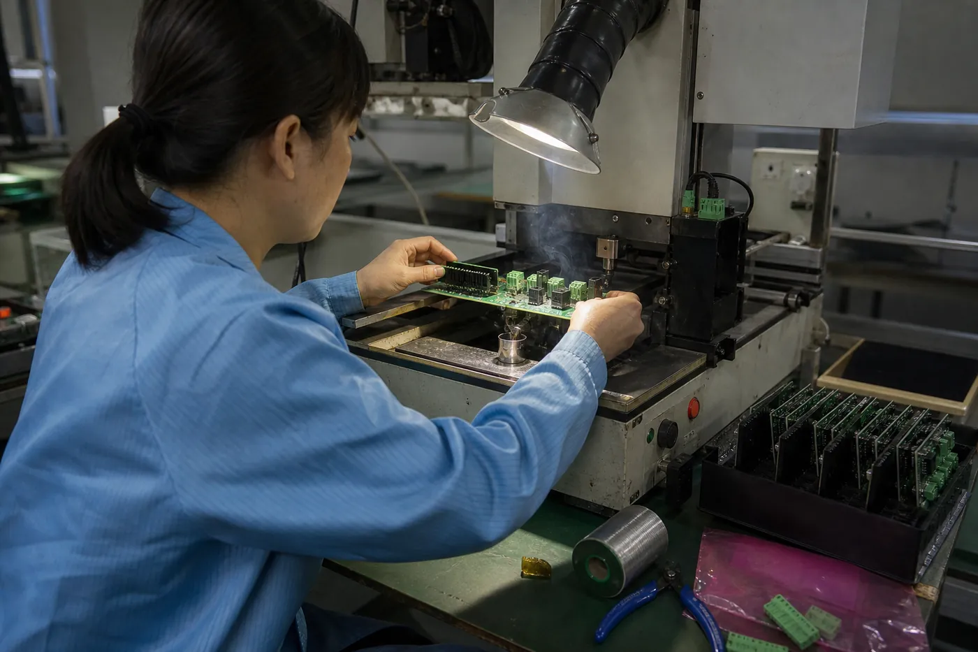
Bare-board incoming inspection
Boards are checked for thickness, warpage, surface finish, hole registration and mask alignment before they are allowed onto the line. Out-of-spec lots are quarantined and reported.
- 05
Stencil fabrication & line setup
A laser-cut, electropolished stencil is produced from the paste layer, and the machine program, feeder carts and nozzle set are prepared for the specific product.
- 06
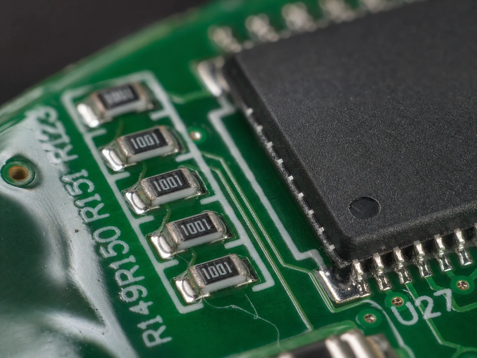
Solder paste printing
Paste is printed in a temperature-controlled room with squeegee pressure and speed set per aperture. The first three prints are measured, not eyeballed.
- 07
3D solder paste inspection
Volume, area, height and offset are measured on every pad. Prints outside the SPC window are washed and reprinted automatically, and the trend is logged per board.
- 08
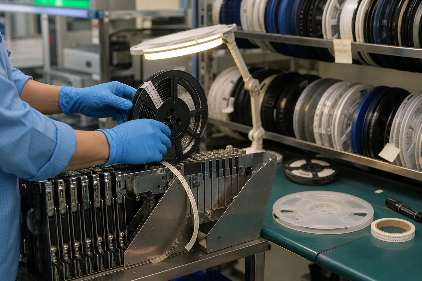
SMT placement
High-speed and fine-pitch heads place passives and ICs in a single pass. On-the-fly vision verifies lead coplanarity and rotation on every fine-pitch device.
- 09
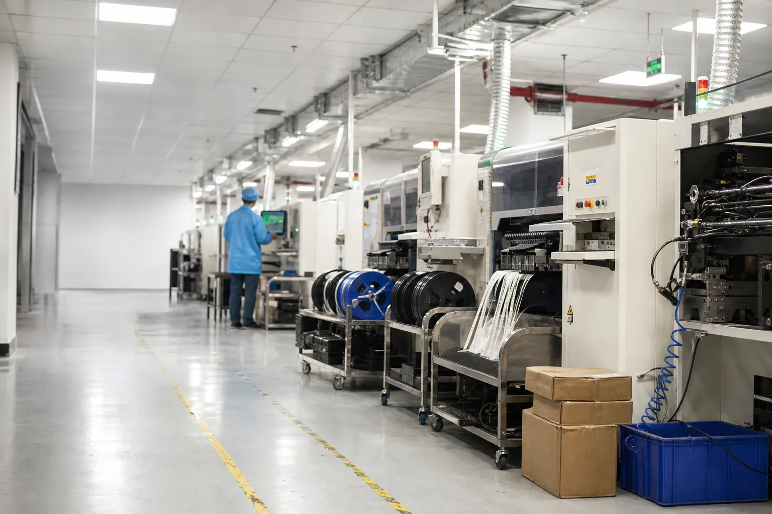
Reflow soldering
Boards pass through a ten-zone nitrogen-purged oven on a profile developed for that assembly. The profile is archived against the product record and re-verified on every run.
- 10
Post-reflow AOI
Every board is optically compared to the golden image. Misalignment, tombstoning, insufficient solder and wrong-polarity parts are caught before test, not after.
- 11
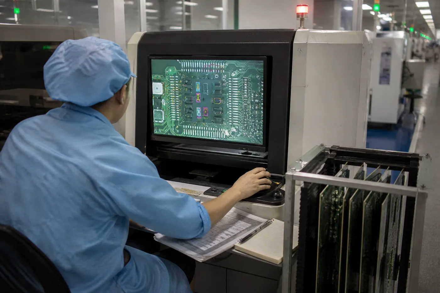
3D X-ray inspection
BGA, CSP and QFN joints are radiographed in 3D. Void percentage and joint geometry are reported per ball against IPC-7095, rather than reduced to a pass or fail.
- 12
THT insertion & selective soldering
Through-hole parts are inserted to an optical template, then soldered by dual-wave or programmable selective nozzle with nitrogen shielding on fine joints.
- 13
Flux cleaning & bake-out
Boards are cleaned where the flux chemistry requires it and baked where moisture uptake matters, with time and temperature recorded for the lot.
- 14
In-circuit test
Flying probe covers prototypes and low volume; a custom bed-of-nails fixture takes over once the product goes to repeat production. Opens, shorts and value drift are all caught here.
- 15
Functional test & programming
A custom jig flashes firmware and exercises the board through its full functional sequence, logging results per serial number. Coverage is agreed with your engineering team before release.
- 16
Coating, potting & box build
Conformal coating, encapsulation, harness assembly and enclosure integration happen on the same site, so the unit leaves as a finished assembly instead of a bare board.
- 17
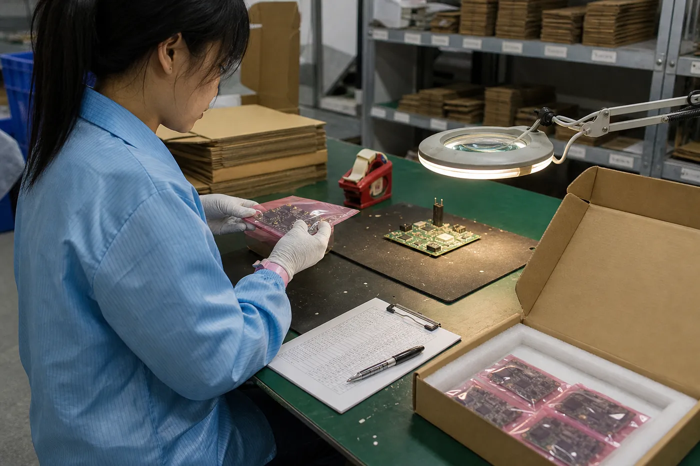
Final QA & outgoing inspection
Workmanship, labelling, quantity and packaging are checked against the drawing. Any deviation found at this gate triggers a written 8D before shipment.
- 18
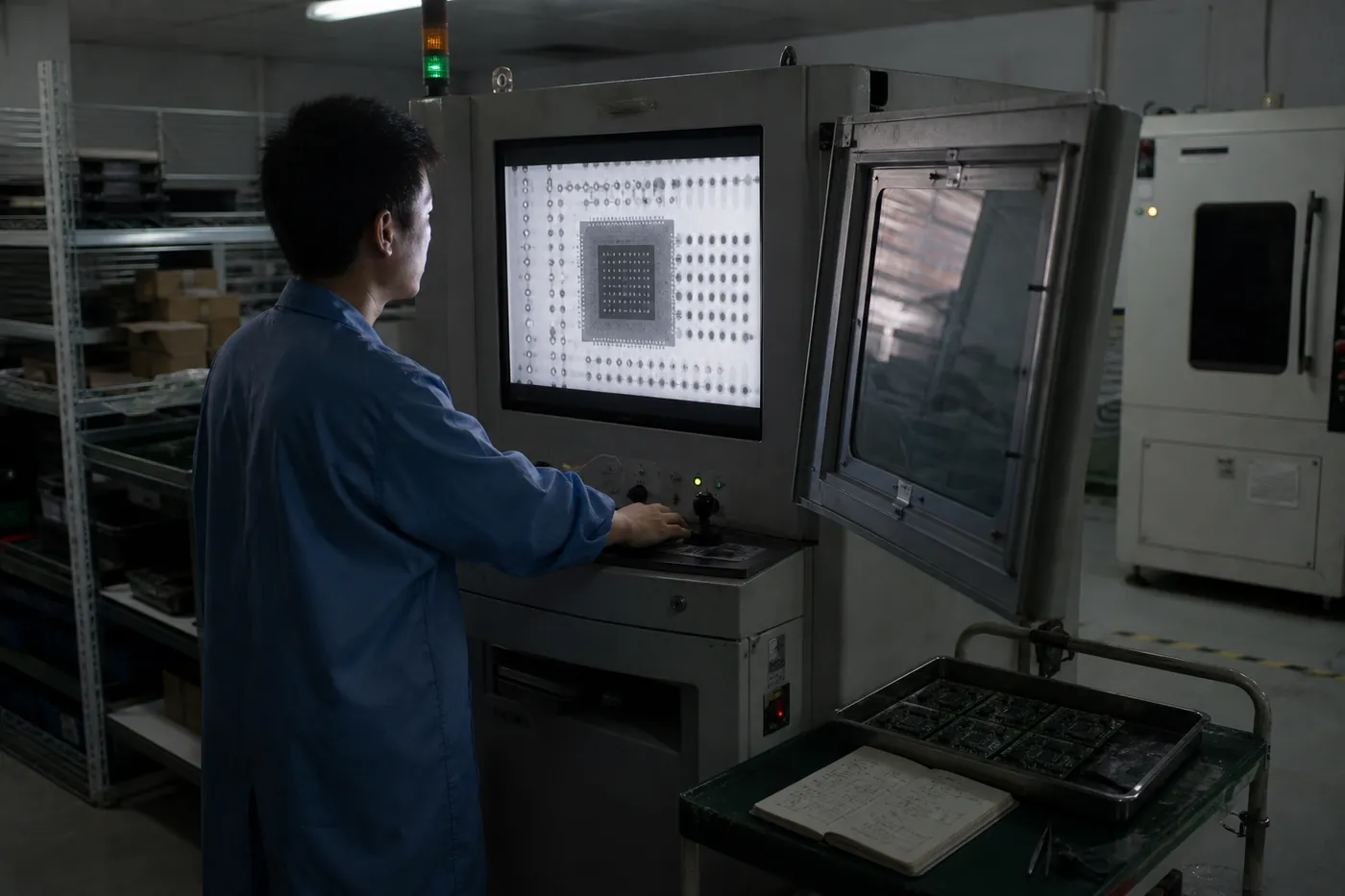
ESD packing & traceability
Boards ship in ESD packaging with desiccant and humidity indicator where required. The certificate of conformance and test log are linked to the production lot and serial range.
Industries we build for
Medical & life sciences
Patient monitoring, diagnostic instruments and laboratory equipment where device history records and serial traceability are mandatory.
Industrial automation
PLC modules, motion controllers and edge gateways built for continuous duty, vibration and wide temperature ranges.
Automotive & EV
Battery management sensing, charging control and telematics boards supplied under PPAP Level 3 discipline.
IoT & consumer devices
Connected sensors, metering nodes and smart hardware moving from pilot batch into repeat production.
Have a design that sits outside the table?
Upload the BOM, centroid file and Gerber. An assembly engineer will confirm feasibility and return an itemized quote — including stencil, fixture and test cost — within 24 hours.